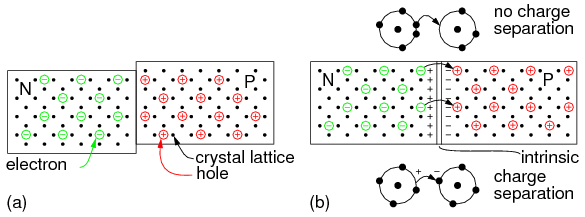
If a block of P-type semiconductor is placed in contact with a block of N-type semiconductor in Figure below(a), the result is of no value. We have two conductive blocks in contact with each other, showing no unique properties. The problem is two separate and distinct crystal bodies. The number of electrons is balanced by the number of protons in both blocks. Thus, neither block has any net charge.
However, a single semiconductor crystal manufactured with P-type material at one end and N-type material at the other in Figure below (b) has some unique properties. The P-type material has positive majority charge carriers, holes, which are free to move about the crystal lattice. The N-type material has mobile negative majority carriers, electrons. Near the junction, the N-type material electrons diffuse across the junction, combining with holes in P-type material. The region of the P-type material near the junction takes on a net negative charge because of the electrons attracted. Since electrons departed the N-type region, it takes on a localized positive charge. The thin layer of the crystal lattice between these charges has been depleted of majority carriers, thus, is known as the depletion region. It becomes nonconductive intrinsic semiconductor material. In effect, we have nearly an insulator separating the conductive P and N doped regions.

(a) Blocks of P and N semiconductor in contact have no exploitable properties. (b) Single crystal doped with P and N-type impurities develop a potential barrier.
This separation of charges at the PN junction constitutes a potential barrier. This potential barrier must be overcome by an external voltage source to make the junction conduct. The formation of the junction and potential barrier happens during the manufacturing process. The magnitude of the potential barrier is a function of the materials used in manufacturing. Silicon PN junctions have a higher potential barrier than germanium junctions.
PN Junction Bias
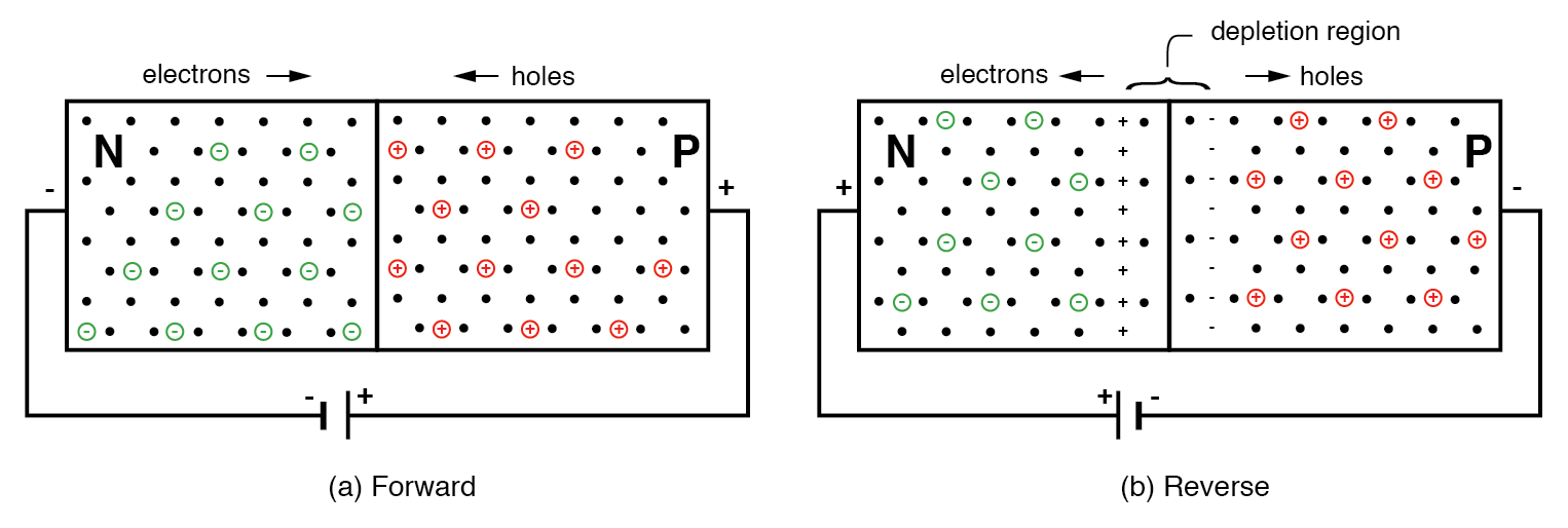
In Figure below(a) the battery is arranged so that the negative terminal supplies electrons to the N-type material. These electrons diffuse toward the junction. The positive terminal removes electrons from the P-type semiconductor, creating holes that diffuse toward the junction. If the battery voltage is great enough to overcome the junction potential (0.6V in Si), the N-type electrons and P-holes combine annihilating each other. This frees up space within the lattice for more carriers to flow toward the junction. Thus, currents of N-type and P-type majority carriers flow toward the junction. The recombination at the junction allows battery current to flow through the PN junction diode. Such a junction is said to be forward-biased.

(a) Forward battery bias repels carriers toward the junction, where recombination results in battery current. (b) Reverse battery bias attracts carriers toward battery terminals, away from the junction. Depletion region thickness increases. No sustained battery current flows.
If the battery polarity is reversed as in Figure above(b) majority carriers are attracted away from the junction toward the battery terminals. The positive battery terminal attracts N-type majority carriers, electrons, away from the junction. The negative terminal attracts P-type majority carriers, holes, away from the junction. This increases the thickness of the nonconducting depletion region. There is no recombination of majority carriers; thus, no conduction. This arrangement of battery polarity is called reverse bias.
Diode
The diode schematic symbol is illustrated in Figure below(b) corresponding to the doped semiconductor bar at (a). The diode is a unidirectional device. Current only flows in one direction, Alongside the arrow, corresponding to forward bias. The cathode, bar, of the diode symbol, corresponds to N-type semiconductor. The anode, arrow, corresponds to the P-type semiconductor. To remember this relationship, Not-pointing (bar) on the symbol corresponds to N-type semiconductor. Pointing (arrow) corresponds to P-type.

(a) Forward biased PN junction, (b) Corresponding diode schematic symbol (c) Silicon Diode I vs V characteristic curve.
If a diode is forward biased as in Figure above(a), the current will increase slightly as the voltage is increased from 0 V. In the case of a silicon diode a measurable current flows when the voltage approaches 0.6 V in Figure above(c). As the voltage increases past 0.6 V, current increases considerably after the knee. Increasing the voltage well beyond 0.7 V may result in high enough current to destroy the diode. The forward voltage, VF, is a characteristic of the semiconductor: 0.6 to 0.7 V for silicon, 0.2 V for germanium, a few volts for Light Emitting Diodes (LED). The forward current ranges from a few mA for point contact diodes to 100 mA for small signal diodes to tens or thousands of amperes for power diodes.
If the diode is reverse biased, only the leakage current of the intrinsic semiconductor flows. This is plotted to the left of the origin in Figure above(c). This current will only be as high as 1 µA for the most extreme conditions for silicon small signal diodes. This current does not increase appreciably with increasing reverse bias until the diode breaks down. At the breakdown, the current increases so greatly that the diode will be destroyed unless a high series resistance limits current. We normally select a diode with a higher reverse voltage rating than any applied voltage to prevent this. Silicon diodes are typically available with reverse break down ratings of 50, 100, 200, 400, 800 V and higher. It is possible to fabricate diodes with a lower rating of a few volts for use as voltage standards.
We previously mentioned that the reverse leakage current of under a µA for silicon diodes was due to the conduction of the intrinsic semiconductor. This is the leakage that can be explained by theory. Thermal energy produces few electron-hole pairs, which conduct leakage current until recombination. In actual practice, this predictable current is only part of the leakage current. Much of the leakage current is due to surface conduction, related to the lack of cleanliness of the semiconductor surface. Both leakage currents increase with increasing temperature, approaching a µA for small silicon diodes.
For germanium, the leakage current is orders of magnitude higher. Since germanium semiconductors are rarely used today, this is not a problem in practice.
REVIEW:
- PN junctions are fabricated from a monocrystalline piece of semiconductor with both a P-type and N-type region in proximity at a junction.
- The transfer of electrons from the N side of the junction to holes annihilated on the P side of the junction produces a barrier voltage. This is 0.6 to 0.7 V in silicon and varies with other semiconductors.
- A forward-biased PN junction conducts a current once the barrier voltage is overcome. The external applied potential forces majority carriers toward the junction where recombination takes place, allowing current flow.
- A reverse-biased PN junction conducts almost no current. The applied reverse bias attracts majority carriers away from the junction. This increases the thickness of the nonconducting depletion region.
- Reverse biased PN junctions show a temperature-dependent reverse leakage current. This is less than a µA in small silicon diodes.